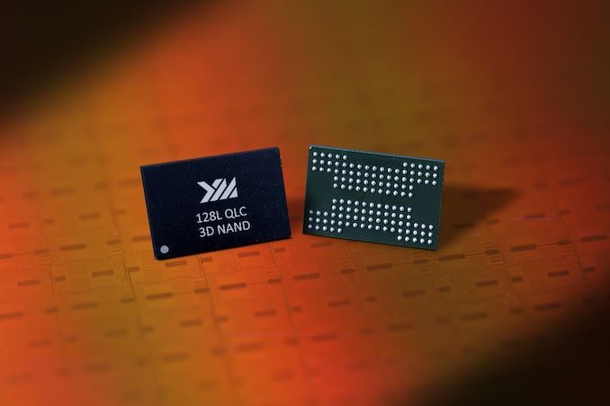
China Develops High Capacity QLC 3D NAND: YMTC at 1.33 Tb
Yangtze Memory Technologies Co. (YMTC) has announced that it's developed its new 128-layer 1.33 Tb QLC 3D NAND memory chip, the X2-6070. The new chip is based on its Xtacking architecture which enables it to run with super high I/O while maximising the density of its memory arrays. YMTC has also unveiled its plan for a 128-layer 512 Gb TLC chip, the X2-9060, designed to meet more diverse application requirements.
We first reported on the China-based company YMTC entering its 3D NAND memory chips into production back in 2018, when it unveiled its Xtacking Architecture at the Flash Memory Summit. While it didn't disclose technical details of its announcement, it did state the Xtacking architecture has the capability to run the I/O with speeds of up to 3 Gbps. Fast forward to 2019, and it announced that it planned to start volume production of its 64-layer 3D NAND which we also reported on.
Using its Xtacking architecture at the forefront of production, both the new X2-6070 and X2-9060 feature its updated 2.0 variant which YMTC claims to bring more benefits to flash memory. Both the X2-6070 and X2-9060 are claimed to deliver up to 1.6 Gb/s of I/O performance and operate with a Vccg voltage of 1.2 V. YTMC has stated that the X2-6070 QLC based chip will be first used in consumer-grade SSDs, with the aim to then deliver its capabilities into Enterprise focused drives.

YMTC X2-6070 128-Layer QLC 3D NAND memory chip
The QLC based X2-6070 has 128-layers and more than 366 billion effective charge-trap memory cells. Each memory cell has 4-bit of data, which equates to 1.33 Tb of storage capacity. Everything is proportionate to cost, and it seems like YMTC, which is newer than most to 3D NAND stacking, could again improve its Xtacking architecture in the future.
We expect that YMTC, who is part of the Tsinghua Unigroup in China, is using the XMC fab in Wuhan China to produce its wafers for its 3D NAND. Tsinghua acquired XMC back in 2016, and while we haven't had it confirmed, it is likely to be producing its wafers at the XMC fab, which is one of China's largest semiconductor fabrication plants which also uses the Xtacking architecture.
YMTC hasn't released official specifications or data sheets about the X2-6070 QLC and X2-9060 MLC memory chips, nor has it stated when it is likely to be integrated with its controller partners (or which controllers support it).
Related Reading
- Yangtze Memory Unveils Xtacking Architecture for 3D NAND: Up to 3 Gbps I/O
- Flash Memory Summit 2018, Yangtze Memory Technology Keynote Live BlogL Unleashing 3D NAND
- YMTC Starts Volume Production of 64-Layer 3D NAND
- SK Hynix Sampling New PCIe 4.0 96L SSDs, 128L 4D NAND Enterprise SSDs
- Micron to Start Volume Production of 128-Layer 3D NAND with RG Architecture This Quarter

Comments
Post a Comment