TSMC: N7+ EUV Process Technology in High Volume, 6nm (N6) Coming Soon
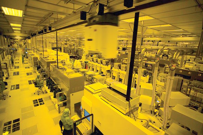
TSMC announced on Monday that its customers have started shipping products based on chips made by TSMC using its N7+ (2nd Generation 7 nm with EUV) process technology that uses extreme ultraviolet lithography (EUVL) for up to four layers. The company also said that its clients are on track to tape out chips to be made using N6 node next year.
When compared to N7 (1st Generation 7 nm) that solely relies on deep ultraviolet lithography, TSMC lists its N7+ process as providing a 15% to 20% higher transistor density as well as 10% lower power consumption at the same complexity and frequency. Furthermore, after less than two quarters in production, TSMC is stating that N7+ now matches N7’s yields, which has been used for over a year now.
Use of EUVL enables TSMC to reduce usage of multipatterning technologies when printing highly complex circuits. This also means that TSMC’s EUV tools can offer output power of greater than 250 watts for day-to-day operations while reaching target goals for availability.
| Advertised PPA Improvements of New Process Technologies Data announced by companies during conference calls, press briefings and in press releases |
|||||||||
| TSMC | |||||||||
| 16FF+ vs 20SOC |
10FF vs 16FF+ |
7FF vs 16FF+ |
7FF vs 10FF |
7FF+ vs 7FF |
6FF vs 7FF |
5FF vs 7FF |
|||
| Power | 60% | 40% | 60% | <40% | 10% | ? | 20% | ||
| Performance | 40% | 20% | 30% | ? | same (?) | ? | 15% | ||
| Area Reduction | none | >50% | 70% | >37% | ~17% | 18% | 45% | ||
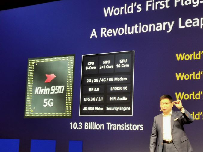
At present, TSMC uses N7+ to produce chips for multiple customers. The most prominent customer of N7+ is Huawei's Hisilicon with the Kirin 990 5G.
TSMC is on track to start risk production of semiconductors using its N6 process technology in the first quarter of 2020 and initiate high-volume production using this node by the end of next year. TSMC’s N6 is a further development of N7 that offers 18% higher transistor density, uses EUVL for up to five layers and enables designers of chips to re-use the same design ecosystem (e.g., tools, IP, etc.), which lowers development costs. By contrast, N7+ uses different design rules, but also provides more benefits than N6 when compared to N7.
Related Reading
- TSMC Announces Performance-Enhanced 7nm & 5nm Process Technologies
- TSMC: Most 7nm Clients Will Transition to 6nm
- TSMC Reveals 6 nm Process Technology: 7 nm with Higher Transistor Density
- TSMC’s 5nm EUV Making Progress: PDK, DRM, EDA Tools, 3rd Party IP Ready
- TSMC: 7nm Now Biggest Share of Revenue
- TSMC: First 7nm EUV Chips Taped Out, 5nm Risk Production in Q2 2019
- TSMC Details 5 nm Process Tech: Aggressive Scaling, But Thin Power and Performance Gains
Source: TSMC


Comments
Post a Comment