SK Hynix Develops First 16 Gb DDR5-5200 Memory Chip, Demos DDR5 RDIMM

SK Hynix on Thursday announced that it had completed development of its first DDR5 memory chip. The new chip offers a capacity of 16 Gb and is said to be the industry’s first DRAM that is fully compliant with the JEDEC standard, which is yet to be published. Meanwhile, mass production of SK Hynix's DDR5 memory chips is slated for 2020.
The new DDR5 chip from SK Hynix supports a 5200 MT/sec/pin data transfer rate, which is 60% faster than the 3200 MT/s rate officially supported by DDR4. Meanwhile the DRAM operates at 1.1 Volts, a 9% decrease in operating voltage. The monolithic 16 Gb chip is made using SK Hynix’s second generation 10 nm-class process technology (also known as 1Ynm), though the company does not disclose its die size and other peculiarities.
Looking forward, SK Hynix expects its DDR5 lineup to include DRAM chips at 8 Gb, 16 Gb, and 32 Gb capacities, with data transfer rates ranging from 3200 to 6400 MT/s.
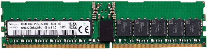
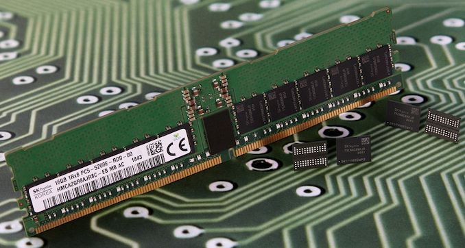
Besides announcing the memory chip, SK Hynix also demonstrated the industry’s first DDR5 Registered DIMM. The DDR5-5200 RDIMM module offers a peak memory bandwidth of 41.6 GB/s, which is in line with DDR4 modules overclocked to their extremes (using LN2-cooled CPUs, etc.). The DDR5 RDIMM itself features 288 pins on a slightly curved edge connector (to reduce the insertion force on every pin), yet its layout and design are a bit different when compared to DDR4 to avoid insertion of DDR5 modules into DDR4 slots and vice versa.
SK Hynix said that it had already shipped DDR5 RDIMMs and UDIMMs to a “major chipset maker” (Intel?) to assist in the development of server and client platforms supporting the new type of memory.
SK Hynix intends to start mass production of DDR5 memory sometimes in 2020, when the aforementioned platforms (at least one of them) are expected to hit the market.
Overall, JEDEC expects DDR5 to bring in I/O speeds ranging from 4266 to 6400 MT/s, with a supply voltage drop to 1.1 V and an allowable fluctuation range of 3% (i.e., at ±0.033V). Along with the performance improvements, the new memory standard also stands to improve in total capacity and DIMM density, with chips planned for 16Gb and beyond.
Under the hood, the new standard will will also bring several major enhancements to the design of memory modules, with the goal of improving their real-world performance and enabling higher data transfer rates. For example, each DDR5 DIMM will feature two independent 32/40-bit channels (without/or with ECC). Furthermore, DDR5 will have a better command bus efficiency (as the channels will have their own 7-bit Address (Add)/Command (Cmd) buses), better refresh schemes, and an increased bank group for extra performance.
Last month Cadence said that enhanced functionality of the standard will enable DDR5 to offer a 36% higher real-world bandwidth vs. DDR4 at the same data transfer rate. While we will not be able to test this claim before 2020, the improvements of DDR5 compared to the predecessor certainly look impressive.
Related Reading:
Cadence & Micron DDR5 Update: 16 Gb Chips on Track for 2019 Cadence and Micron Demo DDR5-4400 IMC and Memory, Due in 2019 JEDEC: DDR5 to Double Bandwidth Over DDR4, NVDIMM-P Specification Due Next YearSource: SK Hynix


Comments
Post a Comment